:
ug472-7Series-Clocking.pdf
资源介绍:
ug472-7Series-Clocking.pdf
7 Series FPGAs
Clocking Resources
User Guide
UG472 (v1.14) July 30, 2018

7 Series FPGAs Clocking Resources User Guide www.xilinx.com UG472 (v1.14) July 30, 2018
The information disclosed to you hereunder (the “Materials”) is provided solely for the selection and use of Xilinx products. To the maximum
extent permitted by applicable law: (1) Materials are made available "AS IS" and with all faults, Xilinx hereby DISCLAIMS ALL
WARRANTIES AND CONDITIONS, EXPRESS, IMPLIED, OR STATUTORY, INCLUDING BUT NOT LIMITED TO WARRANTIES OF
MERCHANTABILITY, NON-INFRINGEMENT, OR FITNESS FOR ANY PARTICULAR PURPOSE; and (2) Xilinx shall not be liable (whether
in contract or tort, including negligence, or under any other theory of liability) for any loss or damage of any kind or nature related to, arising
under, or in connection with, the Materials (including your use of the Materials), including for any direct, indirect, special, incidental, or
consequential loss or damage (including loss of data, profits, goodwill, or any type of loss or damage suffered as a result of any action
brought by a third party) even if such damage or loss was reasonably foreseeable or Xilinx had been advised of the possibility of the same.
Xilinx assumes no obligation to correct any errors contained in the Materials or to notify you of updates to the Materials or to product
specifications. You may not reproduce, modify, distribute, or publicly display the Materials without prior written consent. Certain products are
subject to the terms and conditions of Xilinx’s limited warranty, please refer to Xilinx’s Terms of Sale which can be viewed at
www.xilinx.com/legal.htm#tos
; IP cores may be subject to warranty and support terms contained in a license issued to you by Xilinx. Xilinx
products are not designed or intended to be fail-safe or for use in any application requiring fail-safe performance; you assume sole risk and
liability for use of Xilinx products in such critical applications, please refer to Xilinx’s Terms of Sale which can be viewed at
www.xilinx.com/legal.htm#tos
.
Automotive Applications Disclaimer
AUTOMOTIVE PRODUCTS (IDENTIFIED AS "XA" IN THE PART NUMBER) ARE NOT WARRANTED FOR USE IN THE DEPLOYMENT
OF AIRBAGS OR FOR USE IN APPLICATIONS THAT AFFECT CONTROL OF A VEHICLE ("SAFETY APPLICATION") UNLESS THERE
IS A SAFETY CONCEPT OR REDUNDANCY FEATURE CONSISTENT WITH THE ISO 26262 AUTOMOTIVE SAFETY STANDARD
("SAFETY DESIGN"). CUSTOMER SHALL, PRIOR TO USING OR DISTRIBUTING ANY SYSTEMS THAT INCORPORATE PRODUCTS,
THOROUGHLY TEST SUCH SYSTEMS FOR SAFETY PURPOSES. USE OF PRODUCTS IN A SAFETY APPLICATION WITHOUT A
SAFETY DESIGN IS FULLY AT THE RISK OF CUSTOMER, SUBJECT ONLY TO APPLICABLE LAWS AND REGULATIONS GOVERNING
LIMITATIONS ON PRODUCT LIABILITY.
© Copyright 2011–2018 Xilinx, Inc. Xilinx, the Xilinx logo, Artix, ISE, Kintex, Spartan, Virtex, Vivado, Zynq, and other designated brands
included herein are trademarks of Xilinx in the United States and other countries. PCI, PCIe, and PCI Express are trademarks of PCI-SIG
and used under license. All other trademarks are the property of their respective owners.

UG472 (v1.14) July 30, 2018 www.xilinx.com 7 Series FPGAs Clocking Resources User Guide
Revision History
The following table shows the revision history for this document.
.
Date Version Revision
03/01/2011 1.0 Initial Xilinx release.
03/28/2011 1.1 Updated disclaimer and copyright on page 2. Updated Clocking Architecture Overview
and Figure 2-2. Revised the discussion in Clock-Capable Inputs including adding
Table 1-1 and Figure 2-1. Revised some of the Global Clock Buffers descriptions. Revised
the description under Figure 2-17. Updated the I/O Clock Buffer—BUFIO section.
Updated Figure 2-20. Updated the Regional Clock Buffer—BUFR section. Updated the
description in Table 2-8. Revised Figure 2-23. Added the BUFMRCE to the BUFMR
Primitive section including Figure 2-25. Added BUFHCE to the Horizontal Clock
Buffer—BUFH, BUFHCE section. Moved Clock Gating for Power Savings.
Updated the MMCMs and PLLs section. Revised the Frequency Synthesis Only Using
Integer Divide section including Figure 3-4. Revised the discussion around adjacent
regions in CLKOUT[0:6] – Output Clocks. Updated the examples after Equation 3-11.
Moved and revised VHDL and Verilog Templates and the Clocking Wizard.
Added Appendix A, Multi-Region Clocking.
05/31/2011 1.2 Added section on 7 Series FPGAs Clocking Differences from Previous FPGA
Generations.
Updated Figure 2-2. Clarified discussion in Clock-Capable Inputs section including
removing Table 1-1: Migration of devices in the same package with different top/bottom
alignments. Redrew Figure 2-4, Figure 2-16, Figure 2-18, and Figure 2-22.
Updated description of CLKOUT[0:6] in Table 3-5. Updated CLKFBSTOPPED –
Feedback Clock Status, page 83. Clarified the MMCM/PLL relationship including
updating Figure 3-10. Added more information to the Phase Shift section, including
Equation 3-5.
Revised Figure A-6 and
Figure A-7. Added Appendix B, Clocking Resources and
Connectivity Variations per Clock Region.
10/27/2011 1.3 Moved 7 Series FPGAs Clocking Differences from Previous FPGA Generations. Added
Clock Buffer Selection Considerations. Clarified description in Clock-Capable Inputs.
Added another note after Figure 2-22, page 53. Added the Stacked Silicon Interconnect
Clocking section.
Updated Figure 3-6, page 73. Clarified descriptions in Frequency Synthesis Using
Fractional Divide in the MMCM, page 73, Interpolated Fine Phase Shift in Fixed or
Dynamic Mode in the MMCM, page 75, Determine the Input Frequency, page 76,
CLKOUT[0:6] – Output Clocks, page 82, and Reference Clock Switching, page 91.
Revised description of STARTUP_WAIT, page 85. Updated RST description in Table 3-5,
page 78. Updated CLKOUT[0]_DIVIDE_F(2) allowed values in Table 3-7, page 83.
Updated Clock Network Deskew, page 72 adding Figure 3-12, page 92.
Updated Table B-1 and added Table B-2.
02/16/2012 1.4 Replaced “clocking backbone” with “clock backbone” and “clocking region” with “clock
region” throughout.
Added Chapter 1, Clocking Overview, containing 7 Series FPGAs Clocking Differences
from Previous FPGA Generations from Chapter 2 and Summary of Clock Connectivity
from Appendix B. Updated Table 1-1. Removed XC7A8, XC7A15, XC7A30T, and
XC7A50T from Table 1-2.
Added Clock-Capable Inputs. Updated Global Clocking Resources, including BUFMR
Primitive. Updated Horizontal Clock Buffer—BUFH, BUFHCE. Updated paragraph
before Figure 2-27.

7 Series FPGAs Clocking Resources User Guide www.xilinx.com UG472 (v1.14) July 30, 2018
02/16/2012 1.4
(Cont’d)
In introductory paragraph of High-Performance Clocks, removed description of HPCs
connecting to OSERDES and buffers. Replaced cross reference to UG429, 7 Series FPGAs
Migration Methodology Guide, with UG872
, Large FPGA Methodology Guide. Updated
Stacked Silicon Interconnect Clocking. Replaced SRL with SLR in Figure 2-29. Added
Figure 2-31.
Removed hold block from Figure 3-2. Updated clock frequencies in Frequency Synthesis
Only Using Integer Divide. Replaced 64 with 63 in Equation 3-4. Updated Interpolated
Fine Phase Shift in Fixed or Dynamic Mode in the MMCM. Updated pin description of
LOCKED in Table 3-5. Updated LOCKED. In Table 3-7, updated type and allowed
values of CLKOUT[0]_DIVIDE_F and CLKFBOUT_MULT_F, and description of
STARTUP_WAIT and COMPENSATION. In Table 3-8, added STARTUP_WAIT and
updated description of COMPENSATION. Replaced GTX with GT in Figure 3-10.
Updated Dynamic Reconfiguration Port.
Added Appendix B, Clocking Resources and Connectivity Variations per Clock Region.
07/13/2012 1.5 Updated paragraph after Figure 1-4. Added bullet about spread spectrum support to
Key Differences from Virtex-6 FPGAs. Updated BUFG and BUFH pins, and removed
IBUFDS_GTE2.O/IBUFDS_GTE2.ODIV2 pin from Table 1-1. Updated Table 1-2.
Updated note 5 in Table 2-1. Added Figure 2-29.
Updated last sentence of Introduction. Updated DO[15:0] – Dynamic Reconfiguration
Output Bus. Added SS_EN, SS_MODE, and SS_MOD_PERIOD to Table 3-7. Added
Spread-Spectrum Clock Generation.
10/02/2012 1.6 Added note to Table 1-1. Removed XC7A350T and XC7V1500T from Table 1-2.
Updated first paragraph of Single Clock Driving Multiple CMTs. Added notes 5 and 8 to
Table 2-1. Updated paragraph after Table 2-10.
Added Table 3-9 and timing constraint calculations for 25 MHz and 80 MHz input
clocks. In Table 3-10, changed Bandwidth value from N/A to Low, and removed
duplicate paragraph after table.
Removed XC7A350T from title of Figure B-4.
04/03/2013 1.7 Updated Figure 1-3, Figure B-2, and Figure B-3. Added BUFMR to Table 1-1
. Updated
second paragraph in Dynamic Phase Shift Interface in the MMCM. Added note to
Table 2-7.
08/07/2013 1.8 Updated Table 1-2 and Table 3-7. Updated the figure titles for Figure B-2 and Figure B-3.
Updated Clock Buffer Placement.
04/08/2014 1.9 Updated Clock-Capable Inputs and Dynamic Phase Shift Interface in the MMCM.
Updated allowed values and the default value for CLKFBOUT_MULT in Table 3-8.
05/24/2014 1.10 Changed the value of minimum clock regions from six to four in Clocking Architecture
Overview. Added information to MGTREFCLK0 in Table 1-1. Added section on GTZ
Loopback Clock Buffer — BUFG_LB (HT devices only) to Chapter 2. Changed
description of REF_JITTER1 and REF_JITTER2 in Table 3-7 and Table 3-8. Updated first
paragraph in Use Cases.
11/19/2014 1.11 Removed general interconnect from this bulleted list on page 49. Updated the figure
titles for Figure B-2 and Figure B-3.
03/04/2015 1.11.1 Updated Frequency Synthesis Using Fractional Divide in the MMCM, page 73 by
changing
0.125 degrees to 0.125.
06/12/2015 1.11.2 Fixed broken link in three references to 7 Series FPGA Data Sheets on page 73 and page 74.
09/27/2016 1.12 Added the Spartan-7 FPGAs and the Artix-7 (XC7A12T and XC7A25T) devices where
applicable including updating Appendix B. Updated the BUFR Alignment section.
Updated the Automotive Applications Disclaimer.
Date Version Revision
资源文件列表:
 ug472_7Series_Clocking.pdf 4.12MB
CFA(Chartered Financial Analyst)是全球金融行业内广泛认可的专业资格证书,由CFA Institute颁发。CFA一级考试是整个认证过程的第一步,涵盖了金融基础知识和投资工具等内容。2024年的CFA一级考纲有重大变化,这提示考生需要更加关注新教材和复习材料的更新。
CFA考试的内容每年都会根据金融市场的动态进行调整,以保持其与实际行业的相关性。因此,考生需要了解新考纲中的变动,及时调整学习计划,确保复习的内容符合考试要求。
"2025 notes"通常指的是针对2024年CFA考试的复习笔记或教材,这些材料通常由知名培训机构如Schweser等提供,精炼了官方学习材料,并加入了解题技巧和重点解析。SchweserNotes是CFA备考中广受欢迎的一套辅助资料,它以五本书的形式覆盖了一级考试的所有主题,并包含Quicksheet,这是一种快速回顾关键概念的工具。
北邮数字电路实验
双色点阵扫描显示
测吞吐量和丢包率
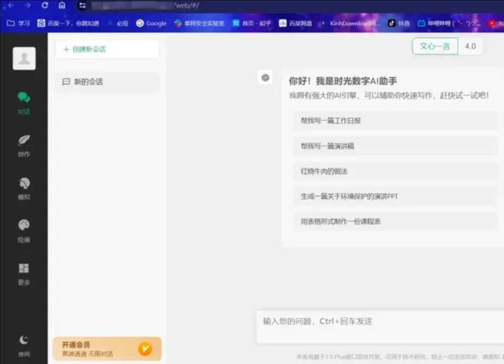
小狐狸GPT付费体验系统的开发基于国外很火的ChatGPT,这是一种基于人工智能技术的问答系统。此版本已经去除授权。可直接安装使用。


带JQUERY效果
主页
及网站建设页


kithara支持的Dlib19.17库
cocos creater2.0 打飞机练习 typescript
Oracle中文基础PPT 虽然是10g,但是学习Oracle,10g版本没问题
Less01_DB_Architecture_MB3.ppt
Less02_Installation_MB3.ppt
Less03_DB_DBCA_MB3.ppt
Less04_Instance_TB3.ppt
Less05_Storage_TB3.ppt
Less06_Users_MB3.ppt
Less07_Schema_TB3.ppt
Less08_Data_TB3.ppt
Less09_Undo_TB3.ppt
Less10_Security_MB3.ppt
Less11_Network_MB3.ppt
Less12_ProactiveM_MB3.ppt
Less13_Performance_TB3.ppt
Less14_BR_Concepts_MB3.ppt
Less15_Backups_TB3.ppt
Less16_R


